
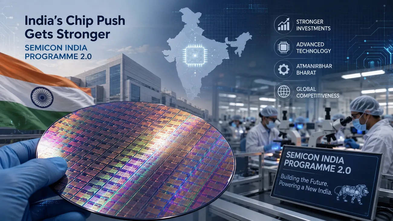
The Indian government has officially notified the Semicon India Programme 2.0 with a massive financial outlay of ₹1.27 lakh crore. Building on the initial phase of the India Semiconductor Mission, this expanded policy aims to deeply integrate the country into the global semiconductor value chain.
By supporting everything from chip design to advanced manufacturing, the initiative seeks to establish a resilient, self-reliant semiconductor ecosystem.
What is Semicon India Programme 2.0?
Semicon India Programme 2.0 is the second phase of India’s national push to build an independent chip-making infrastructure.
It broadens the country’s scope far beyond basic fabrication, offering targeted fiscal backing across the entire semiconductor value chain—including chip design, equipment manufacturing, raw materials, research and development, and talent development.
Why the government increased the outlay
The government expanded its commitment to ₹1.27 lakh crore to transition from initial setup phases to comprehensive, long-term industrial growth.
Global stakeholders have shown rising confidence in India’s technical capabilities, making it the right time to scale up capital support, attract major international investments, and lower vulnerabilities to external supply chain disruptions.
Breakdown of the ₹1.27 lakh crore allocation
The total package is strategically distributed across several critical pillars to ensure balanced development across design, production, and testing:
- Silicon and Specialized Fabs: Core funding dedicated to large-scale semiconductor fabrication plants.
- Packaging and Testing (ATMP/OSAT): Dedicated funds to turn India into an alternative global packaging hub.
- Design Support: Seed capital, risk funding, and deployment-linked incentives for startups and MSMEs.
- Equipment and Materials: Incentives for manufacturing raw chemicals, gases, substrates, and precision components.
- R&D and Talent Creation: Co-funding for advanced technology research and specialized engineering training institutions.
Which semiconductor activities can receive support
The policy covers a wide variety of industrial and academic segments to build a complete domestic loop:
- Commercial and Strategic Chip Design: Focused on domestic startups, MSMEs, and Indian-controlled companies building systems-on-chip (SoCs) and intellectual property.
- Semiconductor Fabrication (Fabs): Including silicon wafer plants, compound semiconductors, sensors, photonics, and display fabs.
- Packaging Facilities: Advanced and legacy packaging, assembly, testing, marking, and packaging (ATMP/OSAT) units.
- Equipment and Raw Materials: Facilities producing specialized machinery, gases, and chemical components.
- Research & Development and Talent: Academic bodies, laboratories, and specialized training programs.
Incentives for fabs, packaging and related facilities
Support levels are tailored across specific segments to optimize capital expenditure (capex) on a pari-passu basis:
| Category | Eligibility & Thresholds | Government Financial Support |
|---|---|---|
| Silicon Wafer Fabs | Min. ₹20,000 crore investment; 300-mm wafers (40,000 starts/month) | Up to 40% of eligible capex |
| Compound / Sensor / Display Fabs | Minimum ₹500 crore investment thresholds | Up to 35% of eligible capex |
| Advanced Packaging (ATMP/OSAT) | Minimum ₹1,000 crore capex and ₹200 crore revenue | 35% for advanced; 25% for legacy packaging |
| Equipment & Materials | Varies by sub-segment (₹50 crore to ₹300 crore thresholds) | Up to 30% capex support plus equipment PLI |
| R&D and Talent Development | Independent or collaborative institutional projects | Up to 75% of project cost |
What has changed from the previous programme
- Broader Ecosystem Reach: While the initial phase focused primarily on getting initial fabrication and basic packaging off the ground, Semicon 2.0 covers six complete pillars, including equipment, raw materials, and deep-tech R&D.
- Targeted Design Support: Introduces robust risk capital, seed funding up to ₹15 crore for startups, and deployment-linked incentives (DLIs) for tape-outs.
- Differentiated Tier Structuring: Offers segmented incentives tailored specifically to distinct tech categories like advanced packaging, compound semiconductors, and display manufacturing.
Also Read: How JioPC Became Available to Everyone in India After the JioHome Restriction
Government’s broader semiconductor strategy
The ultimate objective of the revised framework is to ensure that India captures roughly 10% of the global semiconductor market while anchoring itself securely as an indispensable node in the worldwide supply chain.
By pairing fiscal incentives with continuous workforce development and long-term domestic demand, the strategy lays down the bedrock for a sustainable, 50-year chip industry footprint in the country.
Sources
- [1] The Economic Times — Government notifies Rs 1.27 lakh crore Semicon 2.0 scheme to boost chip ecosystem
- [2] Business Standard — Govt notifies ₹1.27 trillion Semicon 2.0
- [3] Business Today — Semicon 2.0 notified: ₹1.27 lakh crore scheme widens India’s chip ambitions
- [4] The Hindu — IT Ministry notifies semicon scheme’s second phase
- [5] Official India Semiconductor Mission Portal — Semicon 2.0 Guidelines